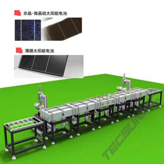
Continuous sputtering line designed for the metallization of amorphous silicon photovoltaic cells on glass substrates in sheet format. The line is intended for integration into thin-film photovoltaic module manufacturing processes and offers the necessary stages to deposit transparent conductive layers, amorphous silicon layers, and electrode metallization by PVD.
Main applications
- Production of photovoltaic glass and amorphous silicon (a-Si) solar cell components in large sheet formats.
- Integration with PECVD processes for deposition of active amorphous silicon layers and with PVD/sputtering for metallic layers.
Process description (typical flow)
- Feeding and transporting the glass sheet through the line in a controlled environment.
- Cleaning and preparing the substrate.
- Deposition of the transparent conductive layer via CVD or PVD depending on the process design.
- Deposition of amorphous silicon layers via PECVD.
- Sputtering metallization to form the aluminum layer or other metallic electrode layers.
- Laser marking/structuring (laser scribing) to define active zones and contacts.
- In-line inspection and electrical tests for quality control.
- Cutting, packaging, and preparation for module assembly.
Advantages for industrial production
- On-line process optimized for roll-to-sheet or sheet-to-sheet manufacturing that reduces operational times.
- Higher utilization of amorphous silicon material and lower production costs compared to crystalline silicon processes, depending on the production process design.
- Compatible with multiple layer configurations (CVD/PVD/PECVD) and subsequent treatments such as laser engraving and automated inspection.
Technical characteristics and integration (typical)
- Modular vacuum system with dedicated PVD sputtering modules.
- Rigid substrate (glass) handling with controlled transport and alignment systems.
- Interface for integration with PECVD equipment and laser/inspection stations.
- Automated process controls, traceability, and in-line testing options.
Why add this line to your plant
- Permits scaling up amorphous silicon cell fabrication with an integrated deposition and metallization solution.
- Facilitates reducing unit costs by optimizing material usage and automating critical steps (deposition, metallization, and scribing).
If needed, we can adapt the technical description to your production requirements (substrate width, production capacity, sputtering target configuration, automation level, and integration requirements with PECVD and testing systems).